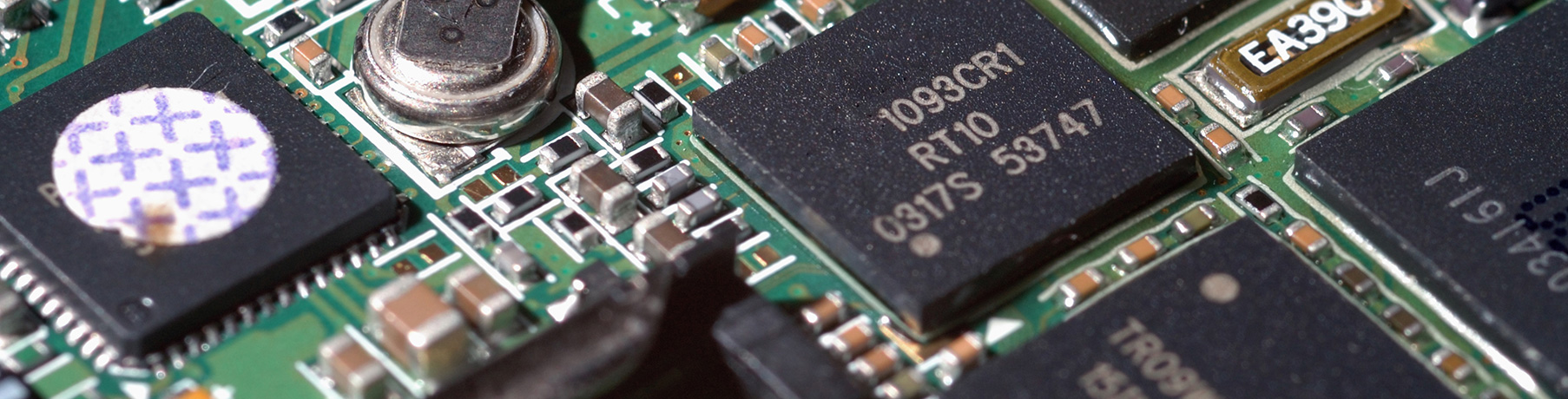
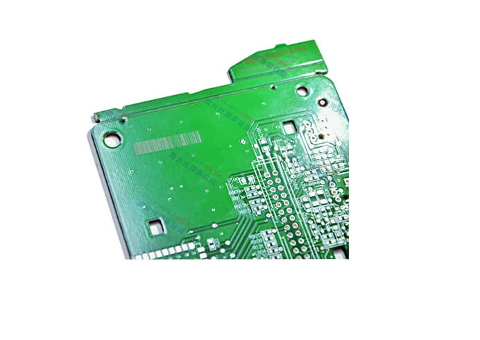
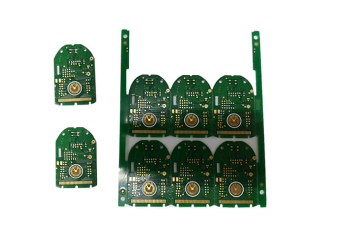
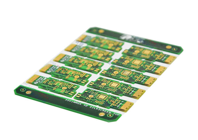
PCBA Depaneling
There are some traditional PCBA singulation methods
Manual PCBA singulation
This method is mainly used on circuit boards with high-stress resistance (for example, there are no SMD parts on the board), and workers can separate the PCBA board along the V groove and a suitable fixture.
Saw blade machine of PCBA
The saw blade can be divided into two types, PCBA boards with and without V grooves.
The saw blade cannot cut multiple materials but can only cut straight PCBA boards. Some dust and stress will also be generated.
The V-cut machine of PCBA
Use the round knife on the V-cut singulation machine or the V-shaped blade on the straight knife to separate the V-slot's PCBA board. The PCBA board can be processed manually, electrically or pneumatically.
Punch machine of PCBA
Punch singulation requires a special punching die to cooperate. Put the PCBA in the proper position of mold, start the punch machine switch. A series of PCBA are cut into small pieces of PCBA boards.
Milling cutting machine of PCBA
The milling cutting machine mainly uses a milling cutter to rotate at high speed to divide a multi-piece rigid PCBA board according to a pre-programmed path. This method solves the limitation that the plate singulation can only be divided into a straight line with a saw blade or V-cut procedures.
Why select Laser?
PCBA laser depaneling PCBA is non-contact process technology, with no mechanical stress, no consumable worn blades, no die cost, no damage to the components, high precision.
Software control, user-friendly, the contour can be easily programmed, and the cutting pattern can be easily defined. The vision system can make accurate marking position recognition. No realignment is required between the switch of different types of panels.
CO2 or UV?
The PCBA cutting speed of the CO2 Laser is faster and at a low cost than UV, but CO2 cutting will have more charring on the cutting edge, and the kerf width is larger than the UV process.
The UV laser is 355 nm wavelength, with a "cold marking" method. The laser beam diameter is only 20 μm after focusing. The pulse energy of the UV laser act on the material is in a microsecond. There is no significant thermal influence next to the slit, so there is no damage to the electronic component caused by the heat generated.
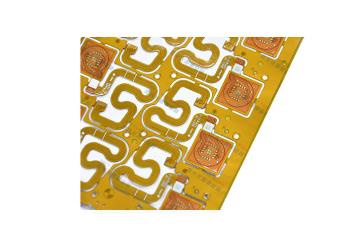
UV Laser is suitable for rigid, flexible and rigid&flexible substrate cutting and marking, like FR4 substrates and imitation resin-based materials, polyimide, ceramics, PTFE, polyester, aluminum, brass and copper, etc.
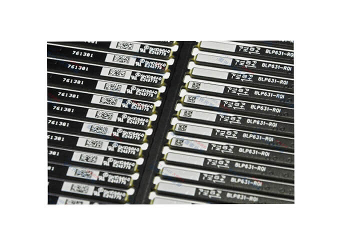
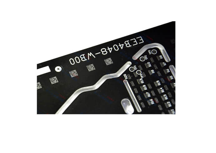
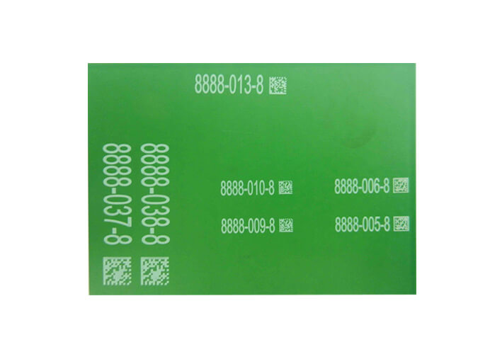
PCB Laser Marking
PCB laser marking can mark various characters, symbols and patterns, etc. The characters' size can range from millimeters to micrometers, which can realize the function of anti-counterfeiting. Besides, laser marking can also process serial numbers and QR codes to record related production information, facilitating the complete traceability and quality control of electronic products.
Compared with traditional inkjet marking, PCB laser marking is more environmentally friendly.
A fully automated PCB Laser marking machine is widely used in the circuit board industry, mainly for assembly line marking operations on integrated circuit boards and semiconductor components, including text or graphic marking. Due to the non-contact processing method, no mechanical pressure is generated. The Laser-focused beam is tiny, which can be used for fine processing of small components, including integrated circuits, crystal oscillators and capacitors.
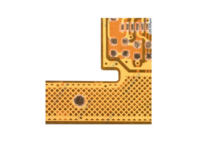
PCB Laser Decoating
In the process of making the PCB board, when the electronic components inserted on the PCB board are tested to be defective, they need to be removed and replaced with a good product. Before replacing a good product, remove the glue that sticks to the defective product on the PCB. The traditional method of Manual grinding or scraping is used, which is time-consuming, laborious and insufficient removal, and the yield of PCB boards after this processing method is not high.
The laser glue removal method is environmentally friendly, no chemical pollution, fast processing speed, it can significantly improve production efficiency.
Tin Ball Laser Soldering
Tin ball laser soldering. After being heated and melted by a laser, the solder balls are ejected from the special nozzle and directly cover the pads. No additional flux or other tools are needed. It is very suitable for processing that requires temperature or soft board connection welding area. During the entire process, the solder joints and the welding body are not in contact, which solves the electrostatic threat caused by contact during the welding process.
Compared with traditional technology, laser solder ball welding has the following advantages:
- The laser processing precision is high, the laser spot is small, the program can control the processing time, and the precision is higher than the traditional process method. It is suitable for the soldering of tiny precision parts and the places where the soldering parts are more sensitive to temperature.
- Non-contact processing, no static electricity caused by welding, can be processed in conventional ways that are not easy to weld.
- A tiny laser beam replaces the soldering iron tip, and it is also easy to process when there are other interference objects on the surface of the processed part.
- Local heating, small heat-affected zone; no electrostatic threat.
- Laser is a clean processing method, simple maintenance, convenient operation, and good stability of repeated operation.
- The heating speed is fast, and the positioning is accurate, which can be completed in 0.2 seconds.
- The tin ball diameter can be as small as 50μm, suitable for high-precision welding.
- The yield rate of solder is higher than that of ordinary automatic soldering machines.
- With a visual positioning system, it is suitable for assembly line production.
PCB Inline/Offline PCB Laser Marking Machine HDZ-PCB100
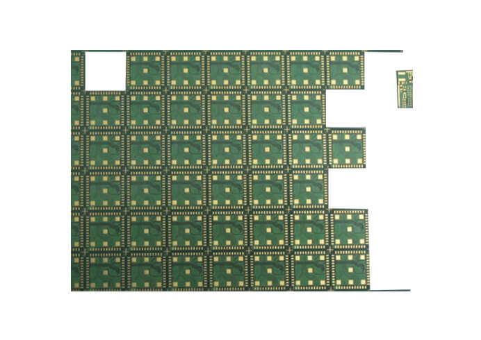
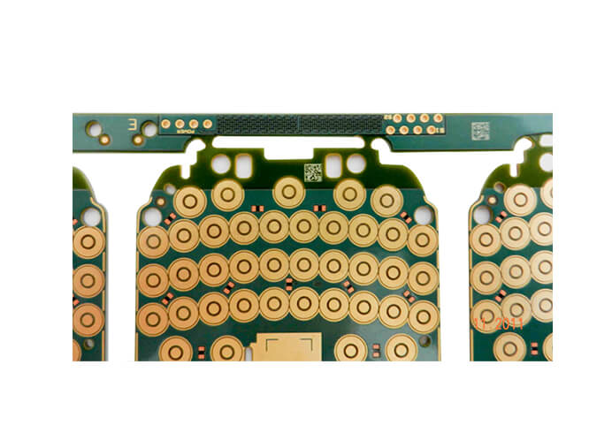
PCBA Laser Depaneling
PCBA Laser Depaneling Machine HDZ-UVC3030
PCB Laser Decoating
We are committed to providing our customers with the latest industrial laser machine technology to suit their particular needs better.
Headquartered in the U.S., employed by knowledgeable, trained personnel. Han's Laser is transforming the industry with our state-of-the-art machines.
Han's Laser Technology Industry Group Co., Ltd, a public company established in 1996, has become the Chinese national laser industry's flagship and one of the world's most famous laser equipment manufacturers. Han's Laser went public in Shenzhen Stock Exchange Market in 2004. And as of today, its market value reaches more than 7 Billion USD.