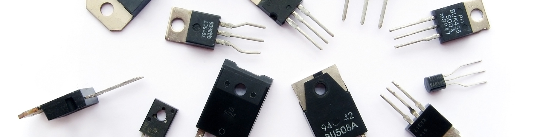
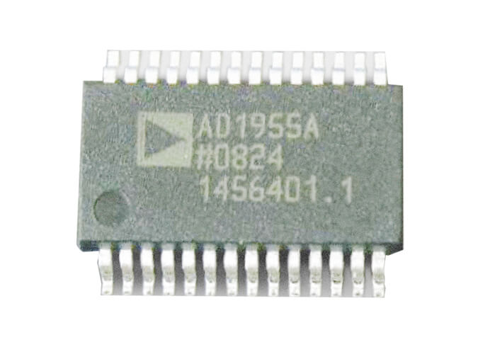
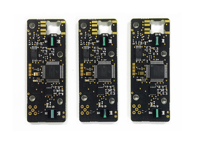
IC Laser Marking
IC is a circuit module that integrates various electronic components on a silicon board to achieve a specific function. There will be some patterns and numbers on the chip's surface for the identification or other procedures. Still, the chip is small in size and high in integration density, so the precision of the chip's surface is very high.
The laser marking machine technology is a non-contact processing method that uses the laser's thermal effect to ablate the surface material of the object to leave a permanent mark. Compared with the traditional electrochemical, silkscreen, mechanical and other marking methods, it is pollution-free and fast. It can mark clear text, model, manufacturer and other information without damaging the components.
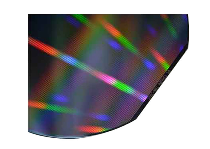
Wafer Laser Marking
A laser is used to print the lot number (such as ABC1234) of the wafer directly above the wafer to ensure the entire process chain's traceability. This lot number is arranged by many recessed holes, a byproduct of marking. It will accumulate around the pits. Excessive or hard protrusions may scratch the wafer's surface in the later process and cause the wafer to be scrapped. Ultraviolet laser processing is a cold processing method that can better solve the problem of accumulation. It is an ideal wafer marking program.
Wafer Laser Dicing
With the improvement of the wafer manufacturing process and the application of carbon powder materials, wafers' hardness has become higher and higher, and the requirements for processing have become higher. The application of laser dicing technology has solved this problem well.
The laser stealth dicing technology is a brand-new laser cutting process that has many advantages: fast cutting speed, no dust, no loss, small cutting path required, and complete dry process.
The main principle of stealth cutting is to focus the short-pulse laser beam through the material's surface and focus it in the middle of the material to form a modified layer in the middle of the material, and then separate the chips by external pressure.
We are committed to providing our customers with the latest industrial laser machine technology to suit their particular needs better.
Headquartered in the U.S., employed by knowledgeable, trained personnel. Han's Laser is transforming the industry with our state-of-the-art machines.
Han's Laser Technology Industry Group Co., Ltd, a public company established in 1996, has become the Chinese national laser industry's flagship and one of the world's most famous laser equipment manufacturers. Han's Laser went public in Shenzhen Stock Exchange Market in 2004. And as of today, its market value reaches more than 7 Billion USD.